SiC : Industrial Ceramic vs Semiconductor Applications
Silicon Carbide (SiC) is a remarkable compound. HMT company supplies 4''6''8'' SiC Wafer include Conductive/Semi-insulated type for semiconductor applications. You can find it in the semiconductor industry market, and advanced ceramics products also rely heavily on it. This often leads the general public to confuse the two as being the same type of product, which is not the case. Silicon carbide can be both a hard and wear-resistant advanced ceramic and a highly efficient and energy-saving semiconductor. Although these two forms share the same chemical composition, they play two entirely different roles in the industrial sector.
Significant differences exist between ceramic-grade silicon carbide and semiconductor-grade silicon carbide materials in terms of crystal structure, manufacturing processes, performance characteristics, and application fields:
1. Raw Material Purity Requirements Differ Significantly
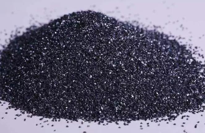 Ceramic-Grade SiC: This has relatively lower purity requirements for the powder. Typically, ordinary industrial-grade products with 90% - 98% purity suffice. However, high-performance structural ceramics may require purities of 98% to 99.5% (e.g., reaction-bonded SiC requires control of free silicon content). It allows for small amounts of impurities and sometimes even intentionally adds sintering aids like aluminum oxide (Al₂O₃) or yttrium oxide (Y₂O₃) to improve sintering performance, helping to lower the sintering temperature and increase the final product's density.
Semiconductor-Grade SiC: This demands near-exacting purity standards for the raw material. Substrate-grade single-crystal SiC requires purity ≥99.9999% (6N), with some high-end applications requiring 7N (99.99999%). Impurity concentrations in the epitaxial layer are typically kept below 10¹⁶ atoms/cm³, especially avoiding deep-level impurities like Boron (B), Aluminum (Al), and Vanadium (V). The reason is that even trace amounts of impurities such as Iron (Fe), Aluminum (Al), or Boron (B) can severely impact its electrical properties. These impurities can cause carrier scattering and reduce the breakdown field strength, thereby affecting the performance and reliability of semiconductor devices. Consequently, impurity concentrations must be strictly controlled.
2. Different Roles and Applications
Ceramic-Grade SiC: The "Industrial Workhorse" primarily serves as a structural material. Leveraging its excellent mechanical properties (high hardness, wear resistance) and thermal properties (high-temperature resistance, oxidation resistance), it excels in applications such as abrasives and grinding tools (grinding wheels, sandpaper), refractory materials (linings for high-temperature kilns/furnaces), and wear/corrosion-resistant components (pump bodies, pipe linings).
Semiconductor-Grade SiC: The "Electronics Elite" utilizes its wide bandgap semiconductor properties to demonstrate
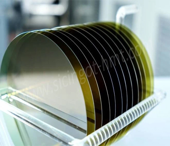 unique advantages in the field of electronic devices. In power devices, such as inverters for electric vehicles or converters for power grids, it enables higher power conversion efficiency and reduces energy loss. In the RF device domain, like 5G base stations and radar systems, semiconductor SiC facilitates higher operating frequencies and stronger signal transmission capabilities. Furthermore, it is used in optoelectronic devices, such as serving as the substrate material for blue LEDs, providing us with bright blue light sources.
CATEGORIES
LATEST NEWS
- Introduction to the main functions of PbootCMS
SiC : Industrial Ceramic vs Semiconductor Applications
- Introduction to the main functions of PbootCMS
How Does AI Help Singe Crystal SiC Boule Growth
- Introduction to the main functions of PbootCMS
Technical Analysis of SiC Wafer For Power Semiconductor Devices in New Energy Vehicles
- Introduction to the main functions of PbootCMS
SiC industry is stepping into 8 inch with 12 inch substrates making accelerated breakthroughs
CONTACT US
Contact: Mr.Kimrui
Phone:
Tel: Please send your detailed inquiry or requirements via email below.
Email: kim@homray-material.com
Add: Please send your detailed inquiry or requirements via email below.