Detailed Explanation SiC Wafer Processing Technology
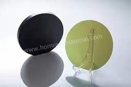
HMT as the leading SiC Wafer Manufacturer will introduce detailed SiC Wafer Processing Technology here for your referene. We supply whole SiC wafer dimension 2inch 4inch 6inch and 8inch with best price. SIC crystal has a high matching with GaN material lattice constant and thermal expansion coefficient and excellent thermal conductivity, is an ideal GaN substrate material, such as LED,LD.
Therefore, the SiC substrate processing technology is an important basis for the production of devices, the quality and accuracy of the surface processing, will directly affect the quality of the epitaxial film and the performance of the device, so the processing of silicon carbide substrate materials requires the surface of the wafer ultra-smooth, no defects, no damage, surface roughness below the nanometer.
1. Raw material preparation
Physical vapor transfer method (PVT) requires Si and C 1:1 synthesis of SiC polycrystalline particle powder, its particle size, purity will directly affect the quality of the crystal, especially the semi-insulated wafer, the purity of the powder is very high (impurity content less than 0.5ppm).
2. Seed crystals
SiC seed crystal is the base of crystal growth, provides the basic lattice structure for crystal growth, and is also the core raw material that determines the quality of crystal. The seed crystals are located inside the reactor or above the feedstock.
3. Crystal growth
SiC crystal growth is the core process of SiC substrate production, the core difficulty is to improve the yield. At present, the main growth methods of SiC crystals are Physical Vapor Transport Method (PVT method) and High Temperature Chemical Vapor Deposition method (High Temperature Chemical Vapor Deposition, High temperature). HTCVD method, Liquid Phase Epitaxy method, etc.
4. Crystal ingot processing
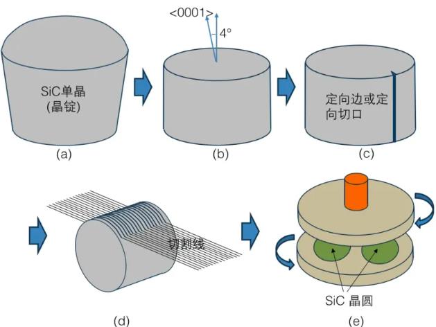
The obtained silicon carbide crystal ingot was orientated by X-ray single crystal orientation instrument, then ground and rounded, removed seed crystal surface and dome surface, and processed into standard diameter SiC crystal.
5, Crystal cutting
The growth of the crystal cut into wafer, because the hardness of sSiC is second only to diamond, belongs to high hard brittle materials, so the cutting process takes a long time, easy to fragment.The main cutting methods are diamond wire multi-wire cutting and laser cutting.

6. Grinding and polishing
Grinding and polishing is to process the substrate surface to an atomically smooth plane. The surface state of the substrate, such as surface roughness and thickness uniformity, will directly affect the quality of the epitaxy process.SiC has the characteristics of high hardness, commonly used for SiC abrasives such as boron carbide, diamond and other high hardness abrasives.
Polishing materials are generally alumina, cerium oxide, silicon oxide and so on.
7. Cleaning and testing
This step is used to remove residual particles and metal impurities during the processing process, and the final detection can obtain comprehensive quality information such as substrate surface, surface shape, crystal quality, and help the downstream process to trace.
CATEGORIES
LATEST NEWS
- Introduction to the main functions of PbootCMS
SiC : Industrial Ceramic vs Semiconductor Applications
- Introduction to the main functions of PbootCMS
How Does AI Help Singe Crystal SiC Boule Growth
- Introduction to the main functions of PbootCMS
Technical Analysis of SiC Wafer For Power Semiconductor Devices in New Energy Vehicles
- Introduction to the main functions of PbootCMS
SiC industry is stepping into 8 inch with 12 inch substrates making accelerated breakthroughs
CONTACT US
Contact: Mr.Kimrui
Phone: 15366208370
Tel: 15366208370
Email: kim@homray-material.com
Add: LiSheng Industrial Building, 60SuLi Road, WuZhong District, JiangSu Province, P.R.China.