Ultrafast Laser Vertical Modification Of SiC Single Crystal Materials
HMT as the SiC Wafer Manufacturer can stable supply 2 inch to 8 inch SiC Wafer and Raw Cut SiC Wafer & SiC Boules, including 4H-N type, 4H-SI type and 4H-P type with best price for different applications. Silicon carbide (SiC), as a typical representative of the third generation semiconductor materials, has been widely used because of its excellent thermal conductivity, wear resistance and corrosion resistance. It has the advantages of high band-gap width, high electron saturation rate and high critical breakdown electric field. These properties make SiC single crystals play a key role in many fields, including semiconductor substrates, microelectronic devices, power electronics, and optoelectronics, especially in harsh environments such as high temperature, high pressure, and high radiation. SiC has become the core material in the transformation and upgrading of important industries such as national defense, 6G communications, and new energy vehicles.
At present, the typical processing processes of SiC single crystal substrates include: single crystal growth, annealing, orientation, grinding, rounding, edging, cutting, chamfering, grinding, polishing and cleaning. Cutting is a key step in the machining process, and parameters such as Bow, Warp and total thickness change (TTV) directly affect the subsequent grinding and polishing processes. At present, the commonly used cutting method on the production line is reciprocating multi-line cutting, but because of the high cost of SiC materials and the short length of the ingot, it is usually necessary to bond multiple ingot for cutting, which is low efficiency and large material loss, resulting in high cost of SiC devices, of which the single crystal substrate material accounts for 50% of the cost of SiC devices.
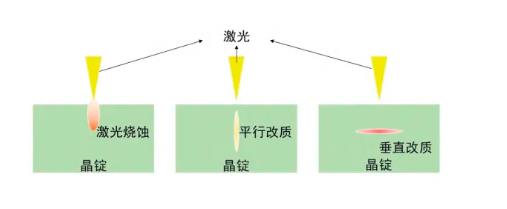
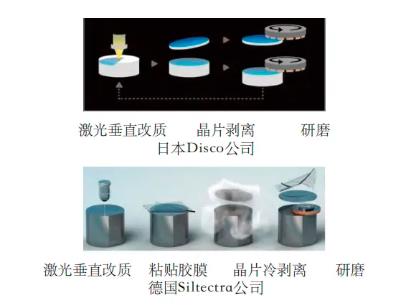
In order to solve this problem, laser vertical modification stripping technology came into being and is considered a revolutionary approach to the challenge of "beyond mole" material processing. This technology can significantly improve the processing efficiency, reduce material loss, and make up for the shortage of multi-line cutting. At present, only the Japanese Disco company and the German Siltectra company have mastered the laser stripping technology for the batch processing of SiC ingot, and the technical routes adopted by the two companies are different. Disco Company developed the KABRA technology of laser induced intracrystal amorphous transformation and realized wafer stripping by mechanical means. The cold cutting technology proposed by Siltectra uses a laser with a high numerical aperture to create microcracks inside the crystal, which are then separated from the remaining ingot through a cooling process.
Industrial-grade ultrafast lasers have extremely high peak power density (>1014 W/cm²), extremely short pulse widths (tens of femtoseconds to 10 picoseconds), and extremely high repetition rates (~1 MHz), which make it extremely difficult to damage and heat affect the material during processing.If the modified layer can be formed inside the SiC single crystal by ultrafast laser, combined with the mechanical stripping process, it can replace the existing cutting method, reduce material loss, reduce costs and shorten the processing time.

CATEGORIES
LATEST NEWS
- Introduction to the main functions of PbootCMS
SiC : Industrial Ceramic vs Semiconductor Applications
- Introduction to the main functions of PbootCMS
How Does AI Help Singe Crystal SiC Boule Growth
- Introduction to the main functions of PbootCMS
Technical Analysis of SiC Wafer For Power Semiconductor Devices in New Energy Vehicles
- Introduction to the main functions of PbootCMS
SiC industry is stepping into 8 inch with 12 inch substrates making accelerated breakthroughs
CONTACT US
Contact: Mr.Kimrui
Phone: 15366208370
Tel: 15366208370
Email: kim@homray-material.com
Add: LiSheng Industrial Building, 60SuLi Road, WuZhong District, JiangSu Province, P.R.China.