
4H-SiC SI Type SiC Wafer Manufacturer
Purchase our 4H-SiC Semi-Insulating (SI) wafers with dimension 4inch to 8inch, the ideal substrate for high-frequency GaN HEMTs, 5G, and radar. Provid...
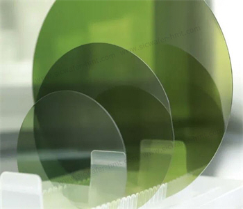
Homray Material's 4H-SiC Semi-Insulating (SI) Wafer represents the standard substrate for high-frequency and high-performance electronic applications. We offer 4 inch 6 inch and 8 inch SI SiC Wafer with D grade R grade and P grade. Growing from 4H silicon carbide polytype ingot, thest wafers are characterized by exceptionally high electrical resistivity, which effectively minimizes signal loss and parasitic capacitance at radio frequencies.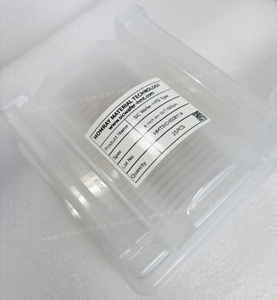
This SI-type SiC wafer serves as an ideal platform for the epitaxial growth of wide-bandgap semiconductors like Gallium Nitride (GaN). Its superior thermal conductivity ensures efficient heat dissipation from power-dense devices, while its excellent crystalline quality guarantees reliability and high yield. This wafer is the foundation of choice for pushing the boundaries of speed and power in modern wireless communication and sensing systems.
Key Features & Applications
4H-SI SiC Wafer Key Features:
High Resistivity: True semi-insulating properties with high electrical resistivity (> 10^5 Ω·cm) for minimal RF signal loss.
Excellent Thermal Management: High thermal conductivity (≥ 4.9 W/cm·K) dissipates heat effectively, enabling stable operation of high-power devices.
Superior Crystalline Quality: Low defect density and micropipes ensure high epitaxial layer quality and superior device performance.
High Hardness and Chemical Inertness: Provides excellent mechanical stability and resistance to harsh processing environments.
Epitaxy-Ready Surface: Precisely polished surface optimized for high-quality GaN or other III-Nitride epitaxial growth.
Semi-insulating SiC Wafer Primary Applications:
RF Electronics: GaN-on-SiC High Electron Mobility Transistors (HEMTs) for radio frequency applications.
5G Infrastructure: Power amplifiers and front-end modules for 5G base stations.
Radar Systems: Components for aerospace, defense, and automotive radars requiring high power and frequency.
High-Frequency Sensors: Sensing devices operating in demanding environments.

CATEGORIES
LATEST NEWS
- Introduction to the main functions of PbootCMS
SiC : Industrial Ceramic vs Semiconductor Applications
- Introduction to the main functions of PbootCMS
How Does AI Help Singe Crystal SiC Boule Growth
- Introduction to the main functions of PbootCMS
Technical Analysis of SiC Wafer For Power Semiconductor Devices in New Energy Vehicles
- Introduction to the main functions of PbootCMS
SiC industry is stepping into 8 inch with 12 inch substrates making accelerated breakthroughs
CONTACT US
Contact: Mr.Kimrui
Phone:
Tel: Please send your detailed inquiry or requirements via email below.
Email: kim@homray-material.com
Add: Please send your detailed inquiry or requirements via email below.