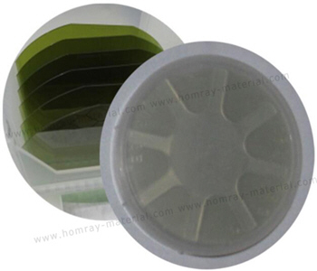
D Grade 8 inch SiC Wafer Manufacturer
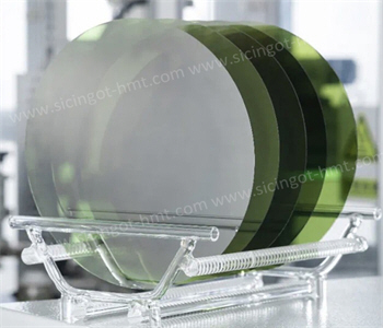
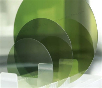
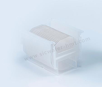
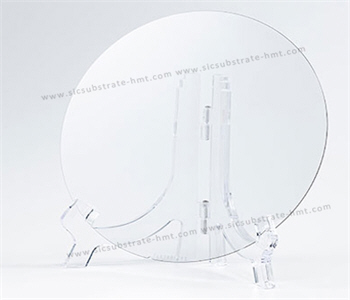
HMT newest and largest D grade 8 inch 4H-N type SiC Wafer has a good price advantage and high quality. We provide both Dummy grade and Production grad...
HMT newest and largest D grade 8 inch 4H-N type SiC Wafer has a good price advantage and high quality. We provide both Dummy grade and Production grade of 8 inch SiC Substrate. HMT provide various types of 4H-SiC Wafers. We have been manufacturer and supplier of SiC wafers to worldwide semiconductor companies and labs for many years. Especially Looking forward to becoming your SiC Wafer long-term supplier in China.
SiC is an important basic material for the development of the third generation semiconductor industry. SiC power devices can effectively meet the requirements of high efficiency, miniaturization and lightweight of power electronic systems with their excellent performance of high pressure, high temperature and low loss.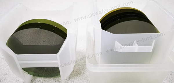
Due to its superior physical properties: high band-gap width (corresponding to high breakdown electric field and high power density), high electrical conductivity, high thermal conductivity, is expected to become the most widely used basic material for making semiconductor chips in the future. In particular, it has obvious advantages in new energy vehicles, photovoltaic power generation, rail transit, smart grid and other fields.
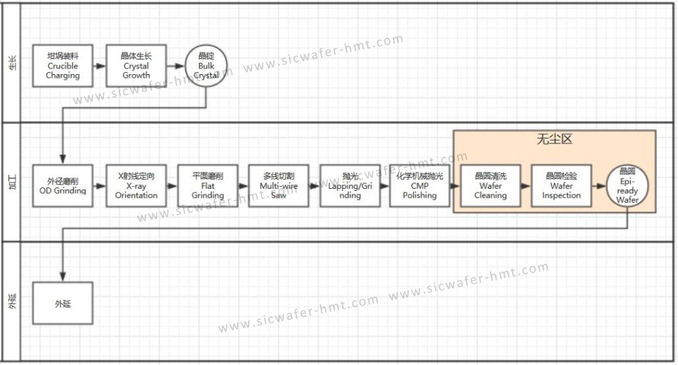
SiC material is difficult to grow in the liquid phase under general conditions, and the vapor phase growth method popular in the market today, the growth temperature is above 2300 ° C, and the growth temperature needs to be precisely regulated, the entire operation process is almost difficult to observe, and a slight error will lead to product scrap. In contrast, silicon materials only need 1600 ° C, which is much lower. The preparation of SIC substrate also faces the difficulty of slow crystal growth and high crystal type requirement. SiC wafer growth takes about 7 to 10 days, while silicon rod pulling takes only 2 and a half days. And SiC is the hardness of the material second only to diamond, cutting, grinding, polishing will also lose a lot, the output ratio is only 60%.
CATEGORIES
LATEST NEWS
- Introduction to the main functions of PbootCMS
SiC : Industrial Ceramic vs Semiconductor Applications
- Introduction to the main functions of PbootCMS
How Does AI Help Singe Crystal SiC Boule Growth
- Introduction to the main functions of PbootCMS
Technical Analysis of SiC Wafer For Power Semiconductor Devices in New Energy Vehicles
- Introduction to the main functions of PbootCMS
SiC industry is stepping into 8 inch with 12 inch substrates making accelerated breakthroughs
CONTACT US
Contact: Mr.Kimrui
Phone: 15366208370
Tel: 15366208370
Email: kim@homray-material.com
Add: LiSheng Industrial Building, 60SuLi Road, WuZhong District, JiangSu Province, P.R.China.
