
Compare SiC Wafer Suppliers: 2025 Price List (50.8mm to 200mm Diameter)
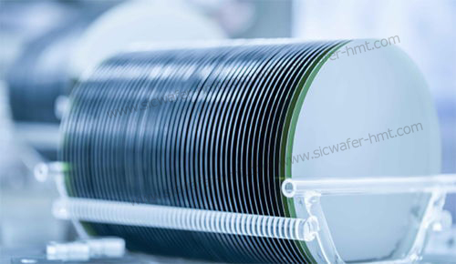
Discover SiC Wafer Supplier Here: HMT 150mm and 200mm SiC substrate wafers with 350um 500um thickness for EV power modules. Explore epitaxial-ready su...
Discover SiC Wafer Supplier Here: HMT 150mm and 200mm SiC substrate wafers with 350um 500um thickness for EV power modules. Explore epitaxial-ready surfaces, P&R&D-grade preferential price with high quanlity. We also supply stop production model of diameter 50.8mm 2 inch SiC Wafers.
Doping Type
N-Nitrogen doped Conducitve type
P-Al doped Conductive type
SI-Un-doped Semi-insulating type
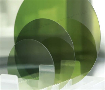
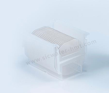
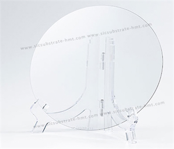
Size & Thickness:
2 inch / 4 inch/ 6 inch/ 8 inch
Thickness 350±25μm/500±25μm,Support Customization
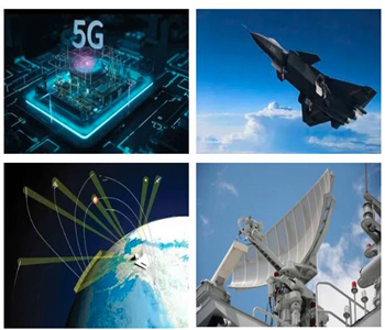
Applications:
EV Power Modules :on-board inverters, DC-DC converters, on-board chargers (OBC)
Renewable energy (PV and wind):Photovoltaic inverter, wind power converter
Industrial power and motor drives:Industrial inverter, servo driver, UPS power supply
5G communication and RF devices:5G base station power amplifier, RF front-end module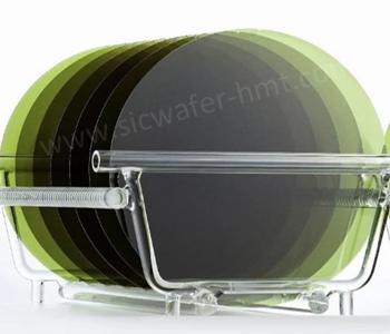

CATEGORIES
LATEST NEWS
- Introduction to the main functions of PbootCMS
SiC : Industrial Ceramic vs Semiconductor Applications
- Introduction to the main functions of PbootCMS
How Does AI Help Singe Crystal SiC Boule Growth
- Introduction to the main functions of PbootCMS
Technical Analysis of SiC Wafer For Power Semiconductor Devices in New Energy Vehicles
- Introduction to the main functions of PbootCMS
SiC industry is stepping into 8 inch with 12 inch substrates making accelerated breakthroughs
CONTACT US
Contact: Mr.Kimrui
Phone:
Tel: Please send your detailed inquiry or requirements via email below.
Email: kim@homray-material.com
Add: Please send your detailed inquiry or requirements via email below.