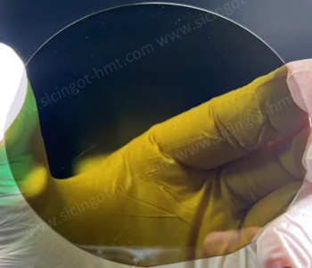
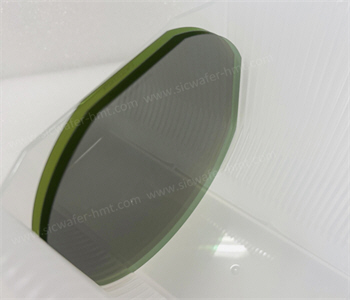
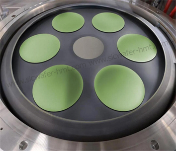
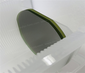
4inch 6inch 8inch SiC-on-SiC Epi Wafer Manufacturer
As the SiC Wafer manufacturer and supplier in semiconductor industry, HMT company can also produce N type and P type 4 inch 6 inch 8 inch SiC Epitaxia...
As the SiC Wafer manufacturer and supplier in semiconductor industry, HMT company can also produce N type and P type 4 inch 6 inch 8 inch SiC Epitaxial on 4H-N type SiC substrate for the development of SiC devices.
What is Epitaxy?
A layer of single crystal thin film material with specific thickness, doping type and concentration, and lattice structure matching with the substrate is grown on the surface of the single crystal substrate carefully processed by cutting, grinding and polishing. This layer of thin film grown is called epitaxial layer, and the whole process is called epitaxial growth.
Different SiC Epitaxial Production Technology
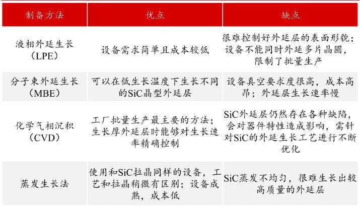
The classification of epitaxy: homogeneous epitaxy and heterogeneous epitaxy
Homogeneous epitaxy: Because of the same material and good lattice matching, the interface between the epitaxy layer and the substrate has high quality and fewer defects. This makes homogeneous epitaxy widely used in manufacturing high performance semiconductor devices, such as high speed integrated circuits, optoelectronic devices, etc. It can precisely control the thickness of epitaxial layer and doping concentration, so as to achieve fine control of device performance.
Heteroepitaxy: Combining the advantages of different materials provides the possibility for the preparation of new devices with special properties. However, due to the lattice constant and thermal expansion coefficient of substrate and epitaxial layer materials are usually different, lattice mismatch and thermal mismatch are easy to occur in the heterogeneous epitaxial process, resulting in defects in the epitaxial layer, which requires high material growth technology and process control.
CATEGORIES
LATEST NEWS
- Introduction to the main functions of PbootCMS
SiC : Industrial Ceramic vs Semiconductor Applications
- Introduction to the main functions of PbootCMS
How Does AI Help Singe Crystal SiC Boule Growth
- Introduction to the main functions of PbootCMS
Technical Analysis of SiC Wafer For Power Semiconductor Devices in New Energy Vehicles
- Introduction to the main functions of PbootCMS
SiC industry is stepping into 8 inch with 12 inch substrates making accelerated breakthroughs
CONTACT US
Contact: Mr.Kimrui
Phone: 15366208370
Tel: 15366208370
Email: kim@homray-material.com
Add: LiSheng Industrial Building, 60SuLi Road, WuZhong District, JiangSu Province, P.R.China.

