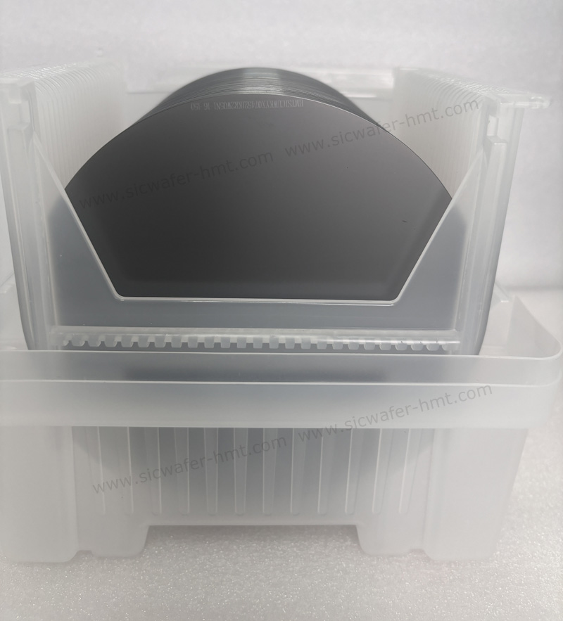
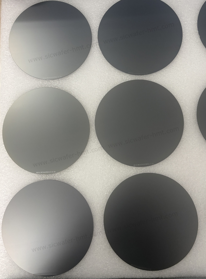
6 inch As Cut SiC Wafer Without lapping and polishing
HMT supplies 6-inch & 8-inch as-cut SiC wafers without lapping/polishing. Optimized for diamond grinding wheels & polishing R&D. Get specs & quote in ...
HMT supplies guaranteed 150mm (6'') and industry-leading 200mm (8'') as-cut SiC wafers without lapping or polishing. Ideal for diamond grinding wheel development, abrasive testing, and next-gen polishing technology R&D, our unprocessed substrates deliver true surface integrity for critical research. While 6 inch unpolished SiC wafers dominate the market, HMT pioneers large-format 8 inch raw slicing wafers – the newest standard for advanced applications.
Fast Delivery: Lead times of 3-5 weeks based on order volume.
Request Details: Contact us today for full technical specifications and competitive quotations on raw SiC substrates – engineered for precision and performance.
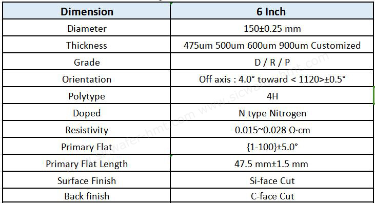
HMT Standard As-cut SiC Wafer Spec:
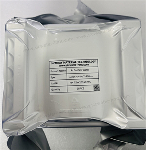
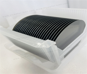
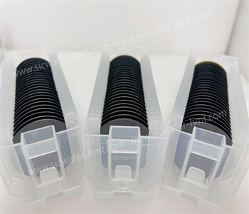
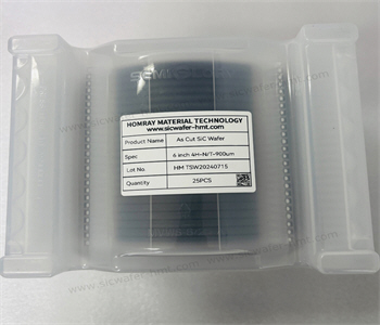
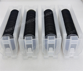
The package of 6 inch Raw Cut SiC wafer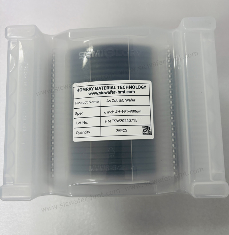
SiC device, the raw material for SiC, according to the different resistance properties, is divided into conductive SiC power devices and semi-insulated SiC based RF devices. The conductive SiC power device is mainly made by growing an epitaxial layer of SiC on a conductive substrate, and obtaining a SiC epitaxial sheet after further processing. Varieties include Schottky diodes, MOSFETs, IGBTs, etc., mainly used in electric vehicles, photovoltaic power generation, rail transit, data centers, charging and other infrastructure fields. The semi-insulated silicon carbon-based RF device is a gallium nitride epitaxial layer grown on the semi-insulated SiC substrate, and the silicon-based gallium nitride epitaxial sheet is prepared and further made, including HEMT gallium iso-nitride RF devices. It is mainly used in 5G communications, vehicle communications, national defense applications, data transmission, aerospace and other fields.
CATEGORIES
LATEST NEWS
- Introduction to the main functions of PbootCMS
SiC : Industrial Ceramic vs Semiconductor Applications
- Introduction to the main functions of PbootCMS
How Does AI Help Singe Crystal SiC Boule Growth
- Introduction to the main functions of PbootCMS
Technical Analysis of SiC Wafer For Power Semiconductor Devices in New Energy Vehicles
- Introduction to the main functions of PbootCMS
SiC industry is stepping into 8 inch with 12 inch substrates making accelerated breakthroughs
CONTACT US
Contact: Mr.Kimrui
Phone:
Tel: Please send your detailed inquiry or requirements via email below.
Email: kim@homray-material.com
Add: Please send your detailed inquiry or requirements via email below.