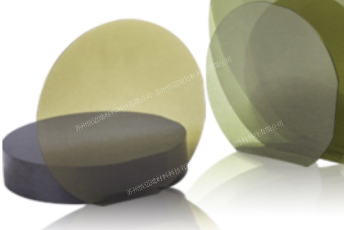
SiC Boules and SiC Substrates industry chain
SiC industry chain is mainly composed of single crystal substrate, epitaxy, devices, manufacturing and testing links. HMT offer the competitive price of 4 inch and 6 inch SiC Boules and SiC wafers with high quanlity. Both Conductive N type and HPSI semi-insualting type are available in HMT. we also support customzied SiC on SiC Epitaxial Wafar upon customers requirements.
In these links, SiC substrate is the key to the development of SiC. The substrate is a wafer made of high-purity polycrystalline SiC powder after sublimation, crystal growth, cutting, grinding, cleaning and other processes. In order to make the material can meet the functional requirements of different chips, it is necessary to prepare different electrical properties of SiC substrate, mainly two kinds: low resistivity conductive SiC substrate, and high resistivity semi-insulating SiC substrate. However, SiC substrates cannot be directly used to manufacture high power and high voltage and high frequency devices. Instead, an additional layer of high quality epitaxial material must be deposited on the single crystal substrate and various devices must be manufactured on the epitaxial layer. A new SiC single crystal layer several microns thick is formed by vacuum evaporation on a polished wafer, which is called epitaxial wafer. Almost all SiC power devices are fabricated based on high quality SiC epitaxial wafers. Epitaxial technology plays a decisive role in the full play of the performance of SiC devices.
Power devices are one of the most important basic components in power electronics industry, which are widely used in electric energy conversion and circuit control of power equipment. The SiC base gallium nitride (GAN-on-sic) epitaxial wafer grown on semi-insulated SiC substrate can be further made into microwave radio frequency devices. Microwave radio frequency devices are the basic components of signal sending and receiving and the core of wireless communication, mainly including radio frequency switches, LNA, power amplifiers, filters and other devices.
The process is similar to that of silicon-based semiconductors, where various SiC devices are manufactured, sealed and tested.
CATEGORIES
LATEST NEWS
- Introduction to the main functions of PbootCMS
SiC : Industrial Ceramic vs Semiconductor Applications
- Introduction to the main functions of PbootCMS
How Does AI Help Singe Crystal SiC Boule Growth
- Introduction to the main functions of PbootCMS
Technical Analysis of SiC Wafer For Power Semiconductor Devices in New Energy Vehicles
- Introduction to the main functions of PbootCMS
SiC industry is stepping into 8 inch with 12 inch substrates making accelerated breakthroughs
CONTACT US
Contact: Mr.Kimrui
Phone: 15366208370
Tel: 15366208370
Email: kim@homray-material.com
Add: LiSheng Industrial Building, 60SuLi Road, WuZhong District, JiangSu Province, P.R.China.