Customized 2 inch SiC Substrate Wafer Supplier
Can you produce 2 inch SiC Substrate wafer now? Of course! HMT as one of professional SiC Wafer Manufacturer and Supplier ,we can still produce stop p...
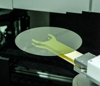
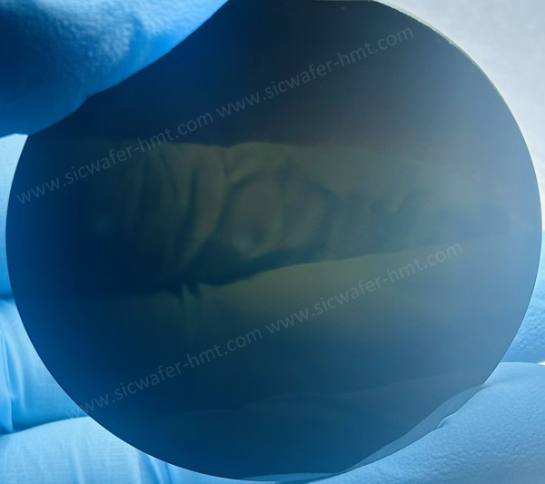
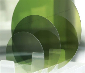
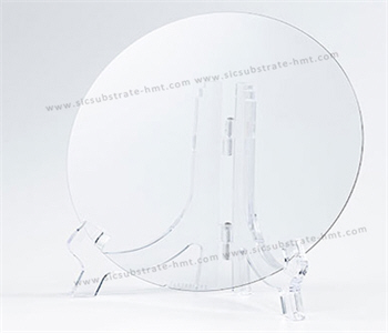
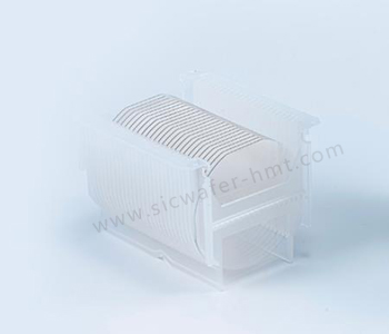
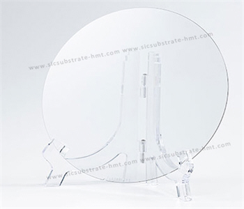
Can you produce 2 inch SiC Substrate wafer now? Of course! HMT as one of professional SiC Wafer Manufacturer and Supplier ,we can still produce stop production model 2 inch 4 inch SiC Wafers, 2 inch As-cut wafers and 2 inch SiC boules. What's more, We can fully customized 2 inch SiC Wafer upon customers different requirements. For example, if you need 2 inch Raw cut SiC wafer thickness>1000um you can contact HMT. If you need 2 inch SiC Substrate thickness 350um TTV < 10um you can contact HMT etc. Don't hesitate to contact us.
2 inch SiC Polished Wafer
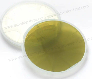
2 inch As cut SiC Wafer
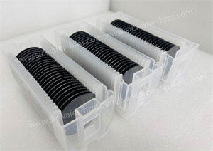
Conductive SiC substrate is mainly used in the manufacture of power devices. Different from the traditional silicon power device manufacturing process, the SIC power device can not be directly fabricated on the SiC substrate, and the silicon carbide epitaxial layer needs to be grown on the conductive substrate to obtain the SiC epitaxial sheet, and the various power devices are manufactured on the epitaxial layer.
CATEGORIES
LATEST NEWS
- Introduction to the main functions of PbootCMS
What Is a TCB Nozzle? Materials, Vacuum Holding and SiC Nozzle Manufacturing
- Introduction to the main functions of PbootCMS
SiC : Industrial Ceramic vs Semiconductor Applications
- Introduction to the main functions of PbootCMS
How Does AI Help Singe Crystal SiC Boule Growth
- Introduction to the main functions of PbootCMS
Technical Analysis of SiC Wafer For Power Semiconductor Devices in New Energy Vehicles
CONTACT US
Contact: Mr.Kimrui
Phone:
Tel: Please send your detailed inquiry or requirements via email below.
Email: kim@homray-material.com
Add: Please send your detailed inquiry or requirements via email below.