4 inch SiC Wafer manufacturers
Homray supplies 100mm 4-inch SiC wafers (4H-N type) for semiconductor R&D & production. Custom thicknesses (350μm/500μm), low MPD/TTV/Bow. Global expr...
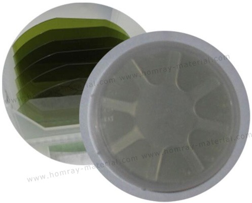
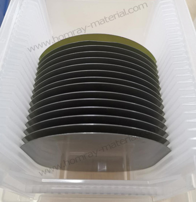
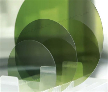
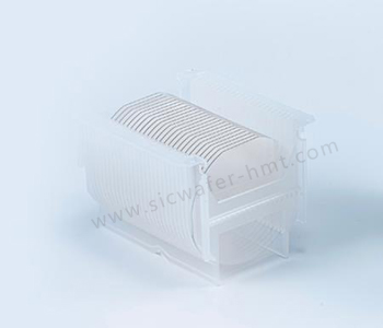
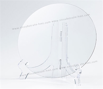
Homray Material Technology (HMT) supplies advanced 4 inch SiC wafers to global semiconductor manufacturers and research laboratories. Our 4'' SiC substrates feature a diameter of 100mm ± 0.25mm and are available in both standard 350μm and customized specifications (e.g., 500μm thickness). Designed as 4H-N type conductive wafers, they deliver superior performance with low Micropipe Density (MPD), minimal Total Thickness Variation (TTV), and controlled Bow. All wafers are securely packaged in industry-standard cassettes and shipped globally via International Express.
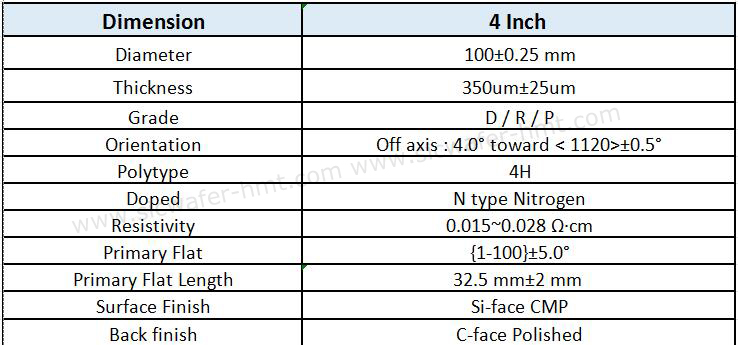
Standard 4'' SiC Substrate Spec
SiC Wafer Application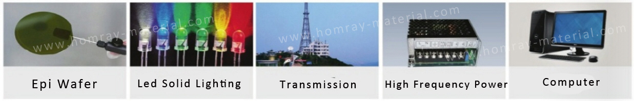
SiC wide energy Gap (Band Gap) than the existing Si (silicon) Gap width more than 3 times wider, can withstand more than 10 times the voltage, SiC low loss, high power characteristics suitable for high voltage and high current application field, including electric vehicles, electric vehicle charging infrastructure, solar energy and offshore wind power and other green power generation equipment.ompared with traditional Si, the third-generation semiconductor material SiC can reduce the power conversion loss by 50%, reduce the power conversion cost by 20%, and improve the endurance of electric vehicles by 4%.

CATEGORIES
LATEST NEWS
- Introduction to the main functions of PbootCMS
SiC : Industrial Ceramic vs Semiconductor Applications
- Introduction to the main functions of PbootCMS
How Does AI Help Singe Crystal SiC Boule Growth
- Introduction to the main functions of PbootCMS
Technical Analysis of SiC Wafer For Power Semiconductor Devices in New Energy Vehicles
- Introduction to the main functions of PbootCMS
SiC industry is stepping into 8 inch with 12 inch substrates making accelerated breakthroughs
CONTACT US
Contact: Mr.Kimrui
Phone:
Tel: Please send your detailed inquiry or requirements via email below.
Email: kim@homray-material.com
Add: Please send your detailed inquiry or requirements via email below.