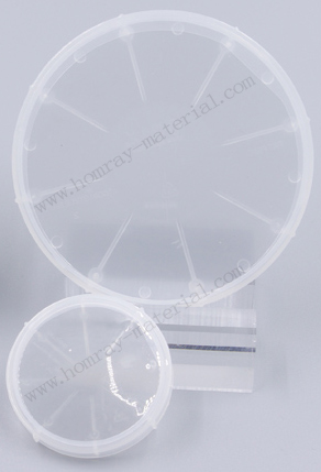
8 Inch HPSI SiC Wafer Manufacturer for AR Glasses and Optical Waveguides
HMT supplies high-purity semi-insulating 8 inch SiC wafers for AR glasses and optical waveguide applications. Our 200mm silicon carbide substrates fea...
8 Inch HPSI SiC Wafer Manufacturer for AR Glasses and Optical Waveguides
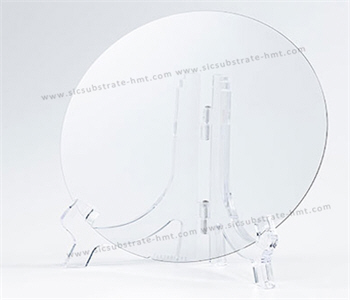
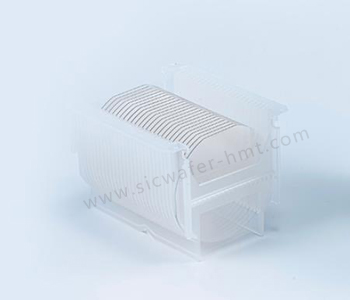
HMT is a professional 8 inch SiC wafer manufacturer specializing in high-quality HPSI silicon carbide (SiC) substrates for advanced optical and semiconductor applications. Our 200mm semi-insulating SiC wafers are designed for next-generation AR glasses, augmented reality displays, optical waveguides, photonics, and high-performance electronic devices.
High-purity semi-insulating silicon carbide (HPSI SiC) wafers are becoming an advanced substrate material for next-generation AR glasses, augmented reality displays, and optical waveguide systems.
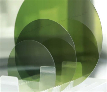
Compared with traditional glass and other optical substrate materials, silicon carbide (SiC) wafers offer superior optical and thermal properties, making them an ideal platform for high-performance AR optical components.
With a high refractive index of approximately 2.7, SiC enables compact optical designs with improved light coupling efficiency, wider field of view, and enhanced image quality for augmented reality applications.
Our 8 inch SiC wafers feature excellent crystal quality, high purity, superior thermal conductivity, and customizable specifications to meet different optical and semiconductor manufacturing requirements.
Why Choose SiC Wafer for AR Glasses and Optical Waveguides?
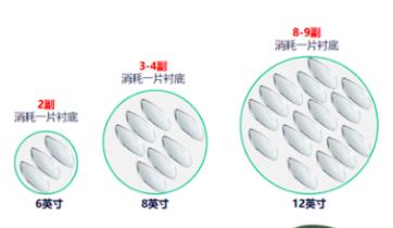
The development of next-generation AR glasses requires optical materials with high refractive index, excellent thermal management capability, and reliable manufacturing performance.
Silicon carbide wafers provide several key advantages compared with conventional optical substrates.
1. High Refractive Index for Improved AR Optical Performance
One of the major advantages of SiC substrate materials is their high refractive index.
The refractive index of silicon carbide is significantly higher than traditional glass materials, allowing AR waveguide designers to achieve:
Larger field of view
Improved optical efficiency
More compact optical modules
Better light transmission performance
For advanced AR glasses and augmented reality waveguide applications, high-index HPSI SiC wafers provide an effective solution for improving optical system performance.
2. Excellent Thermal Conductivity and Device Reliability
AR optical systems often integrate compact optical engines and electronic components that generate heat during operation.
Silicon carbide wafers have excellent thermal conductivity, helping efficiently dissipate heat and improve the stability and reliability of optical devices.
The superior thermal characteristics of SiC substrates make them suitable for demanding applications requiring long-term performance and consistent optical quality.
3. Large Diameter 8 Inch Wafer Platform for High Volume Manufacturing
The transition from small diameter substrates to 8 inch (200mm) SiC wafers enables higher production efficiency and improved manufacturing economics.
Compared with smaller wafer sizes, 200mm SiC wafers provide:
Higher device output per wafer
Better production efficiency
Reduced manufacturing cost
Compatibility with advanced semiconductor processes
HMT's 8 inch HPSI SiC wafers are designed to support future high-volume production requirements for AR optical components and semiconductor devices.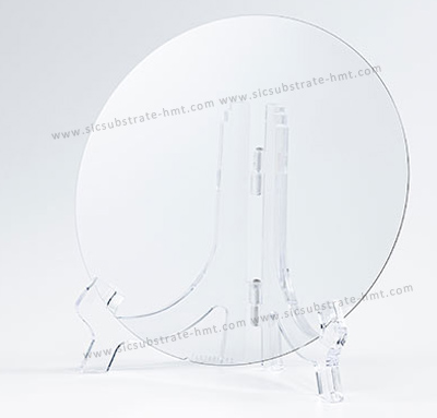
8 Inch HPSI SiC Wafer Specifications
HMT supplies high-quality 8 inch semi-insulating SiC wafers with customized specifications for optical and semiconductor applications.
| Parameter | Specification |
|---|---|
| Material | Silicon Carbide (SiC) |
| Wafer Diameter | 8 inch / 200mm |
| Crystal Structure | 4H-SiC |
| Conductivity Type | HPSI Semi-Insulating |
| Resistivity | >1×10⁷ Ω·cm |
| Surface Finish | Polished / CMP |
| Thickness | Customized according to customer requirements |
| Application | AR Glasses, Optical Waveguides, Photonics, Semiconductor Devices |
| Customization | Available |
What is an HPSI SiC wafer?
An HPSI SiC wafer (High Purity Semi-Insulating Silicon Carbide wafer) is a high-resistivity SiC substrate commonly used for RF devices, optical applications, and advanced semiconductor technologies.
Its excellent electrical insulation properties and material stability make it suitable for high-performance applications.
Do you supply customized 8 inch SiC wafers?
Yes. HMT provides customized 8 inch HPSI SiC wafers with different thicknesses, polishing specifications, and technical requirements according to customer application needs.
CATEGORIES
LATEST NEWS
- Introduction to the main functions of PbootCMS
What Is a TCB Nozzle? Materials, Vacuum Holding and SiC Nozzle Manufacturing
- Introduction to the main functions of PbootCMS
SiC : Industrial Ceramic vs Semiconductor Applications
- Introduction to the main functions of PbootCMS
How Does AI Help Singe Crystal SiC Boule Growth
- Introduction to the main functions of PbootCMS
Technical Analysis of SiC Wafer For Power Semiconductor Devices in New Energy Vehicles
CONTACT US
Contact: Mr.Kimrui
Phone:
Tel: Please send your detailed inquiry or requirements via email below.
Email: kim@homray-material.com
Add: Please send your detailed inquiry or requirements via email below.