4 inch SiC Substrates Manufacturer|High-Yield, Great Price
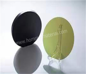
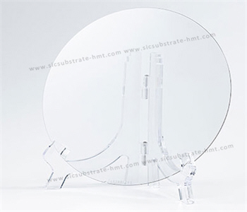
HMT is 4 inch(4H-N) SiC Substrates Manufacturer and Company. HMT can produce any customizing SiC substrates thickness (500um 800um) upon your projects...
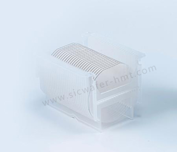
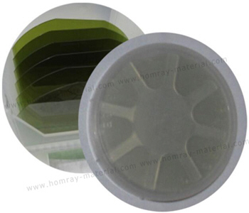
4 inch(4H-N) SiC Substrates Manufacturer HMT provides 4''6''8'' conductive sic substrates with high cost effectiveness for domestic and foreign customers in batches. HMT's 4 inch SiC substrates deliver unmatched reliability and efficiency in demanding power electronics and radio frequency (RF) applications. Not only 4 inch SiC Substrate,we also provide 6 inch and 8 inch 4H semi insulating Wafers. Engineered with ultra-low defect density (<0.5 cm⁻²) these substrates enable faster time-to-market for electric vehicles (EVs), industrial motor drives, and 5G/6G infrastructure.
 Key Features of 4-Inch SiC Substrates
Cost-Effective Scalability
Ideal for mid-volume production and R&D, reducing upfront costs while maintaining compatibility with legacy 4 inch fabrication tools.
Supports both 4H-SiC and 6H-SiC crystal structures, tailored for MOSFETs, Schottky diodes, and RF amplifiers.
Ultra-Smooth Surface Quality
Surface roughness <0.2 nm Ra (epi-ready), ensuring flawless epitaxial growth for GaN-on-SiC Epitaxy wafers and SiC-on-SiC devices.
Broad Industry Compatibility
SiC SubstrateTechnical Specifications
Diameter: 100mm (4 inches)
Thickness: 350µm ±25µm (thickness customizable)
Crystal Type: 4H-SiC (semi-insulating or conductive)
Resistivity: 0.015–0.025 ohm·cm/≥1E5ohm.cm (adjustable doping)
Join industry pioneers leveraging our SiC substrates to slash energy losses by 50% and double power density in critical systems. Request a quotation or datasheet today to experience the precision of next-level SiC innovation!
CATEGORIES
LATEST NEWS
- Introduction to the main functions of PbootCMS
SiC : Industrial Ceramic vs Semiconductor Applications
- Introduction to the main functions of PbootCMS
How Does AI Help Singe Crystal SiC Boule Growth
- Introduction to the main functions of PbootCMS
Technical Analysis of SiC Wafer For Power Semiconductor Devices in New Energy Vehicles
- Introduction to the main functions of PbootCMS
SiC industry is stepping into 8 inch with 12 inch substrates making accelerated breakthroughs
CONTACT US
Contact: Mr.Kimrui
Phone: 15366208370
Tel: 15366208370
Email: kim@homray-material.com
Add: LiSheng Industrial Building, 60SuLi Road, WuZhong District, JiangSu Province, P.R.China.


